Granite River Labs, GRL
Dennis Lan
To say that electronic devices have become indispensable to the modern world would be an understatement. Widespread USB interfaces that transfer data between electronic devices are vital for facilitating work and play, and demand for USB power supply capabilities are only increasing each year.
How Qualcomm Quick Charge 2.0 revolutionized power supply capabilities
In response to rising demand, power supply capability of USB technology has continuously evolved to keep pace with demand. USB 2.0's power supply capability of 2.5W (5V@0.5A) was raised to 4.5W (5V@0.9A) with the advent of USB 3.0. Likewise, the power supply capability of BC 1.2 supported products also increased to 7.5W (5V@1.5A). But the real breakthrough in power supply capabilities came with the introduction of Qualcomm's Quick Charge (QC) technology.
In 2014, Qualcomm introduced Quick Charge 2.0 (QC 2.0) with a power supply capability of up to 60W (20V@3A)¹, almost eight times the wattage of its predecessors. The subsequent release of Quick Charge 3.0 (QC 3.0) ushered in continuous mode along with stepped adjustment characteristics², providing a wider range of voltage options for power supply of QC technology, which we will be exploring in this article.
How does HVDCP support QC 2.0 and QC 3.0?
Qualcomm's High Voltage Dedicated Charging Port (HVDCP) is a type of fast charging device that does not have USB data transfer capabilities. However, HVDCP can communicate with portable devices and negotiate the voltage level for power supply.
The power supply capability of HVDCP can be divided into two classes:
- Class A offers a power supply capability of 5V, 9V, and 12V
- Class B requires support for 20V voltage in addition to 5V, 9V, and 12V
All HVDCPs that support QC 3.0 must be backward compatible with QC 2.0, making it a versatile and efficient charging solution.
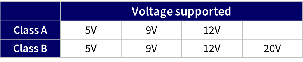
Table 1: Supported Power Voltage for Class A & B HVDCP
Detecting HVDCP in Quick Charge supported devices
Charging with HVDCP is only possible when both the portable device and charging port supports Quick Charge. The portable device initiates the detection process, which involves three steps similar to those specified in the BC 1.2 specification:
- VBUS Detect: When the portable device connects to HVDCP and detects that the VBUS voltage is greater than the internal valid voltage threshold VOTG_SESS_VLD (0.8-4V), it means that the portable device is connected to a valid circuit.
- Primary Detection: HVDCP will short the D+ / D- above it through RDCP_DAT, and the portable device will supply a voltage VDP_SRC (0.6V) on D+, and compare the voltage on D- (VDM) with VDAT_REF (0.25-0.4V). If VDM is greater than VDAT_REF, it means that the HVDCP supports BC1.2. Then, by detecting whether the D+ voltage is greater than VDAT_REF for a period of time TGLITCH_BC_DONE (1-1.5s), the portable device can confirm whether it can complete the BC1.2 detection procedure.
- The third step is unrelated to BC1.2: HVDCP will disconnect D+/D- and turn on RDM_DWN to inform the portable device that this HVDCP supports QC. Finally, after the D- voltage is maintained below VDAT_REF Min (0.25V) for a period of time TGLITCH_DM_LOW (1ms), the HVDCP can start to respond to the voltage request raised by the portable device.

Figure 1: HVDCP (High Voltage Dedicated Charging Port) Circuit Diagram
What are the differences in power supply capabilities of QC 2.0 vs QC 3.0?
There is little difference in the power supply capabilities of HVDCPs that support QC 2.0 and QC 3.0. As with QC 3.0 HVDCP, QC 2.0 HVDCP is also categorized into Class A and Class B, with Class A supporting power supply of 5V, 9V, and 12V, and Class B supporting 20V. The main distinction between the two is that QC 2.0 HVDCP lacks Continuous mode support, and by extension lacks the ability for making stepped adjustments to the VBUS voltage output like the QC 3.0 HVDCP.
What happens when different voltages are requested from a portable device?
Once the D- voltage is held below VDAT_REF for a period of time TGLITCH_DM_LOW (1ms), the HVDCP can start responding to different voltage mode requests from the portable device. Charging is requested by the portable device through switching different D+/D- levels, where the high level is 3.3V and the low level is 0.6V.
These levels are divided by VSEL_REF (approximately 2V) into 3.3V (VUP) and 0.6V (VSRC). When the portable device requests charging, the HVDCP begins adjusting the VBUS output voltage after a period of TGLITCH_MODE_CHANGE (20-60ms) and completes the VBUS switching within TV_NEW_REQUEST (200ms) to attain the VBUS voltage requested by the portable device.
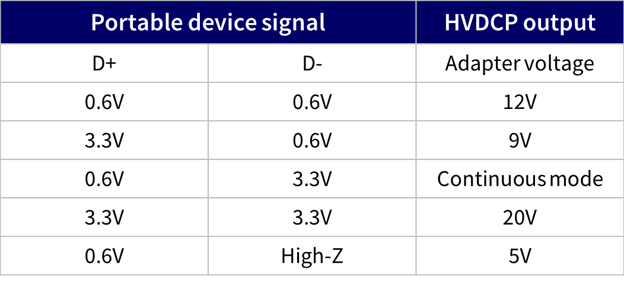
Table 2: D+/D- voltages with the corresponding HVDCP outputs
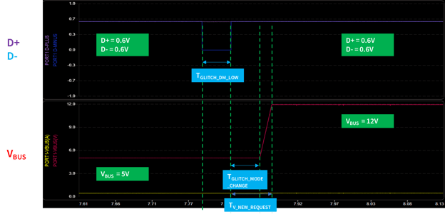
Figure 2: 12V request from portable device
Continuous mode supported by QC 3.0
In Continuous mode, the portable device can control the VBUS voltage output by sending D+ and D- pulses. To enter Continuous mode, the portable device sets D+ to 0.6V and D- to 3.3V, and after a period of time TGLITCH_MODE_CHANGE (20-60ms), it enters Continuous mode.
A D+ pulse briefly raises D+ from 0.6V to 3.3V and then lowers it back to 0.6V, resulting in a 0.2V increase in VBUS voltage. A D- pulse briefly lowers D- from 3.3V to 0.6V and then raises it back to 3.3V, resulting in a 0.2V decrease in VBUS voltage. Portable devices can emit multiple D+ or D- pulses at once, with each pulse resulting in a 0.2V change in VBUS voltage.
After the last pulse is sent, the HVDCP must raise or lower the VBUS to the final voltage value within TV_CONT_CHANGE (2ms) from the rising edge of the last D+ pulse (if D+ rises to 3.3V) or the falling edge of the last D- pulse (if D- falls to 0.6V).
The rising edge or falling edge shall be within TGLITCH_CONT_CHANGE (100-200µs) for an effective pulse, and as long as it meets this requirement, it will raise or lower the VBUS voltage.
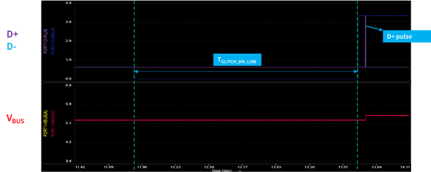
Figure 3: Continuous mode request from portable device
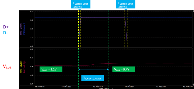
Figure 4: Amplified D+ Pulse from Figure 3
Determining the maximum output current of HVDCP using power profile
Using the power profile, we can determine the maximum output current of an HVDCP at different voltages. To examine the output of a Class A HVDCP that supports QC 3.0, we must examine the two power profile mechanisms (Figure 5) demarcated by Region A (below 6V) and Region B (above 6V). It can be seen that in Continuous mode, the maximum output current that can be delivered is 3A at a voltage of 3.6-6V. This means that this HVDCP can deliver a maximum wattage of 18W (6V/3A).
As the voltage increases beyond 6V, the current will decrease to maintain the total wattage below or equal the maximum wattage. The two power profiles shown below represent different ways in which the current decreases. In Figure 5, the current decreases in a stepped manner as the voltage increases, and the wattage does not reach the maximum. In contrast, in Figure 6, as the voltage increases, the current decreases smoothly while maintaining the maximum wattage.
If the HVDCP operates in Region B, it must be able to return to a maximum output current of 3A when the voltage switches back to Region A.
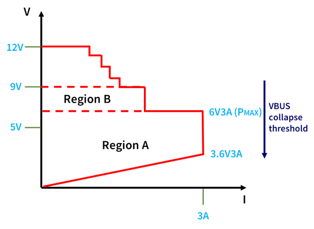
Figure 5: Power profile of Class A HVDCP
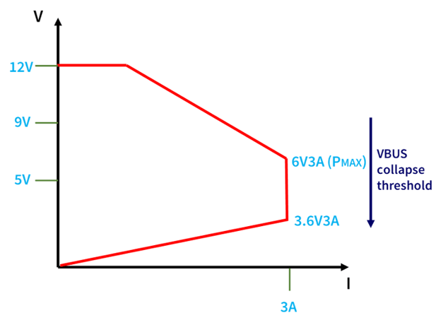
Figure 6: Constant power profile of Class A HVDCP
What happens when the current exceeds the HVDCP’s limit?
When the current drawn by a portable device exceeds the maximum current that the HVDCP can supply at a particular voltage as defined in the power profile, the HVDCP must initiate a protective mechanism known as "Collapse." In Collapse, the HVDCP lowers the voltage output below a certain threshold point (as shown in Table 3) and maintains it for TGLITCH_UVLO (20ms). This informs the portable device that the maximum current that the HVDCP can supply at that voltage has been exceeded. Once Collapse is triggered, the HVDCP cannot switch the output voltage or reduce the output current until the portable device reduces its power demand to a level that is within the HVDCP's power profile.
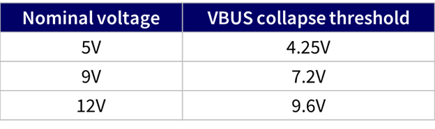
Table 3: VBUS Collapse thresholds
Qualcomm Quick Charge specifications at a glance
The Quick Charge 2.0 and 3.0 fast charging specifications developed by Qualcomm includes a comprehensive power supply mechanism and has greatly improved power supply capabilities up to 60W (20V 3A) compared to the original BC1.2 specification of 7.5W (5V 1.5A). While the BC1.2 architecture required portable devices to detect the HVDCP and request different voltage requirements by adjusting the D+/D- voltage, including 5V, 9V, 12V, and 20V, QC 3.0 enables voltage step adjustments to be achieved using D+/D- pulses. Whenever the portable device draws more current from the HVDCP than the maximum current it can supply at a particular voltage, the HVDCP has a complete Collapse mechanism that lowers the voltage below a certain threshold (see Table 3) and maintains TGLITCH_UVLO (20ms) to let the portable device know its power supply capabilities.
Test and certify your Quick Charge products at GRL
GRL is a third-party lab authorized by Qualcomm to provide Quick Charge test services and Quick Charge automatic test solutions. In addition, we also have experts who specialize in USB interfaces and charging technologies and can provide USB PD certification testing services. If you have any queries or require assistance with charging technology specifications, we are available to help. Please feel free to contact us.

References
- High Voltage Dedicated Charging Port, QuickCharge 2.0 Interface Specification, March 27, 2014
- High-Voltage Dedicated Charging Port, Qualcomm® Quick Charge™ 3.0 Interface Specification 2017
/%E5%BF%AB%E5%85%85%E6%8A%80%E8%A1%93%EF%BC%9AUSB%20Power%20Delivery%20%E5%92%8C%20Quick%20Charge%E2%84%A2%20%E4%BB%8B%E7%B4%B9_featured%20image.jpeg)