Granite River Labs, GRL
郄雅楠 Josie Qie
PCI Express, or PCIe (Peripheral Component Interconnect Express), is a high-performance and high-bandwidth serial communication standard that has become the key interface for servers and PCs since its introduction in 2003. PCIe offers improved system throughput, scalability, and flexibility at a lower production cost. Figure 1 illustrates how PCI-SIG, the electronics industry consortium responsible for formulating PCIe, achieves higher data throughput rates by continuously improving on transmission speeds throughout the years.
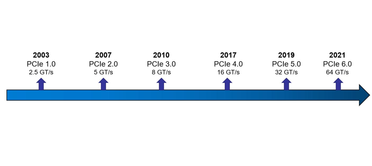
Figure 1: Evolution of PCIe data throughput rates and standards from 2003 to 2021
But with increased signal transmission rates comes an increased risk for signal loss during transmission. Factors such as channel quality and transmission rate can contribute to interference that distort the receiver's ability to capture signals accurately. Beyond a certain threshold, signal distortion can result in high error rates that ultimately impact communication performance. To make up for this inevitable distortion, signal compensation is applied at both the transmitter and receiver ends. This compensation process is known as PCIe link equalization and aims to strengthen incoming PCIe signals that will in turn build clear signal eye diagrams.
How PCIe link training has evolved over the years
Earlier interactions of PCIe (PCIe 1.0 and PCIe 2.0) saw physical mediums constructed out of FR4 PCB material and inexpensive connectors. Adopting 8b/10b encoding and fixed de-emphasis equalization at the transmitter was enough to ensure the quality of low signal throughput, eliminating the need for PCIe equalization parameter negotiation. As a result, PCIe equalization processes were more straightforward and standardized in the early days.
- PCIe 1.0: De-emphasis value fixed at -3.5dB.
- PCIe 2.0: De-emphasis value fixed at -3.5dB and -6dB, without dynamic adjustment.
However, as data speeds increased to and beyond 8.0GT/s from PCIe 3.0 onwards, ensuring PCIe signal integrity during the transmission phase using traditional de-emphasis methods alone became virtually impossible. Instead, the strategy of negotiating equalization coefficients between the transmitter and receiver was adopted, and optimal transmission performance was achieved once more.
To maintain compatibility with previous generations that still used traditional FR4 PCB material and inexpensive connectors, PCI-SIG has introduced two important enhancements to the specifications beyond PCIe 3.0:
- Replacing 8b/10b encoding with 128b/130b encoding: This updated encoding scheme significantly improves encoding efficiency, enabling higher data rates to be transmitted more effectively.
- Adoption of dynamic equalization technology: Also known as Link Equalization (LEQ), dynamic equalization technology replaces static equalization to allow for flexibility when adjusting equalization settings so that the receiver can obtain an optimal eye diagram.
PCIe 3.0, PCIe 4.0, and PCIe 5.0 link equalization
Conducted after link training, link equalization helps establish a stable and efficient connection between PCIe devices. Link equalization optimizes links by adjusting transmitter (Tx) and receiver (Rx) settings to achieve stable, high rate PCIe links. Link equalization is applicable to devices supporting PCIe 3.0 and above. As each generation requires unique settings to optimize connections, the link equalization between each unique set of PCIe devices may require multiple rounds of troubleshooting before an optimal link is attained.
For instance, links between PCIe 5.0 devices require three link equalization processes: the first from PCIe 1.0 to PCIe 3.0, the second from PCIe 3.0 to PCIe 4.0, and the third from PCIe 4.0 to PCIe 5.0. Link equalization uses preset values defined in the PCIe specification, where each preset represents a different combination of pre-shoot and de-emphasis values. For PCIe 3.0 and PCIe 4.0, there are 11 preset values, labeled as preset0 to preset10.
The system will request the Rx terminal to send Tx EQ preset setting requests to the Tx terminal based on corresponding preset equalization settings. In turn, the Tx terminal will send Rx EQ equalization settings back for further adjustments. Through this negotiation process, an optimal combination of equalization presets is achieved, resulting in an improved Rx eye diagram and overall link performance.
During link equalization phases 0-3, the preset values are negotiated between upstream and downstream ports until the optimal settings for both transmitter (Tx) and receiver (Rx) sides are determined. As a result, the link operates with a low bit error rate (BER) of ≤ 1E-12. The negotiation process takes place at both the electrical sub-block and the logical sub-block, with the position of link equalization within the PCIe architecture shown in Figure 2.
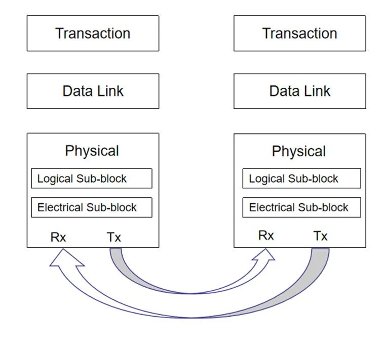
Figure 2: Architecture of Link Equalization in PCIe
PCIe link negotiation at the electrical sub-block
Tx equalization
- Pre-emphasis: In high-speed PCIe serial communication signals, signal distortion occurs due to greater attenuation of high-frequency components compared to low-frequency components, especially at the signal's rise and fall edges. Pre-emphasis compensates for the attenuation of high-frequency components by increasing the signal amplitude at the transition edges, effectively boosting the high-frequency components.
- De-emphasis: Since high-frequency signal components experience greater attenuation than low-frequency components, de-emphasis reduces the signal amplitude outside the transition edges, thereby mitigating the impact of low-frequency components.
- Feed-forward Equalizer (FFE): FFE is typically implemented using finite impulse response (FIR) filters, which add delayed signals of varying weights. Adjusting weight values allows equalization strength to be controlled. FFE enhances the high-frequency components in the signal to achieve channel loss compensation.
Rx equalization
- Continuous-Time Linear Equalizer (CTLE): CTLE is similar to a passive high-pass filter. It suppresses the low-frequency components of the signal, resulting in a smaller amplitude difference between the high-frequency and low-frequency components. The drawback is that it attenuates the low-frequency components of the signal and amplifies high-frequency noise in the transmission system, potentially worsening the signal-to-noise ratio.
- Decision Feedback Equalizer (DFE): Positioned after the linear equalizer, DFE is a nonlinear equalizer consisting of two transversal filters and a decision device. The two transversal filters are the Feed Forward Filter (FFF) and the Feedback Filter (FBF). DFE is used in cases where the eye diagram needs to be opened. Unlike CTLE, DFE doesn't amplify high-frequency noise. However, it can only address post-cursor interference and cannot eliminate pre-cursor interference. It is also more complex in design and consumes more power.
FFE and CTLE are capable of reducing most of the jitter caused by intersymbol interference, while DFE provides further mitigation of intersymbol interference and some reflections caused by impedance mismatches. Combining these equalization techniques helps to enhance signal quality and improve overall system performance.
PCIe link negotiation at the logical sub-block
The Link Training and Status State Machine (LTSSM), as shown in Figure 3, is a part of the logical sub-block in the PCIe physical layer.

Figure 3: Transitions between substates within LTSSM (Source: PCI-SIG)
Dynamic equalization negotiation takes place during the Recovery substate of LTSSM, allowing for the link’s equalization settings to be flexibly adjusted. This process optimizes the TX EQ and enables simultaneous adjustment of RX EQ at both local and remote ends. Dynamic balancing allows systems to flexibly adapt to changing channel conditions.
The basic process of initial equalization after power-up follows a sequence of Detect - Polling - Configuration - L0 - Recovery, operating at a speed of 2.5GT/s. In the polling state, both the Upstream Port (USP) and Downstream Port (DSP) declare support for speeds of 8GT/s and higher. As a result, the USP (or DSP) initiates a speed change request, followed by an equalization request initiated by the DSP (or USP). The speed change and equalization process commence during the Recovery state.
PCIe dynamic link equalization
During the link training process, the dynamic negotiation of transmitter (Tx) and receiver (Rx) parameters takes place in the Recovery.Equalization substate within the LTSSM. This negotiation of equalization coefficients occurs in four phases: Phase 0-3 (DSP: Phase 1-Phase 3; USP: Phase 0-Phase 3), as well as the optional Phase 2 and Phase 3. The transitions between Recovery substates are shown in Figure 4.
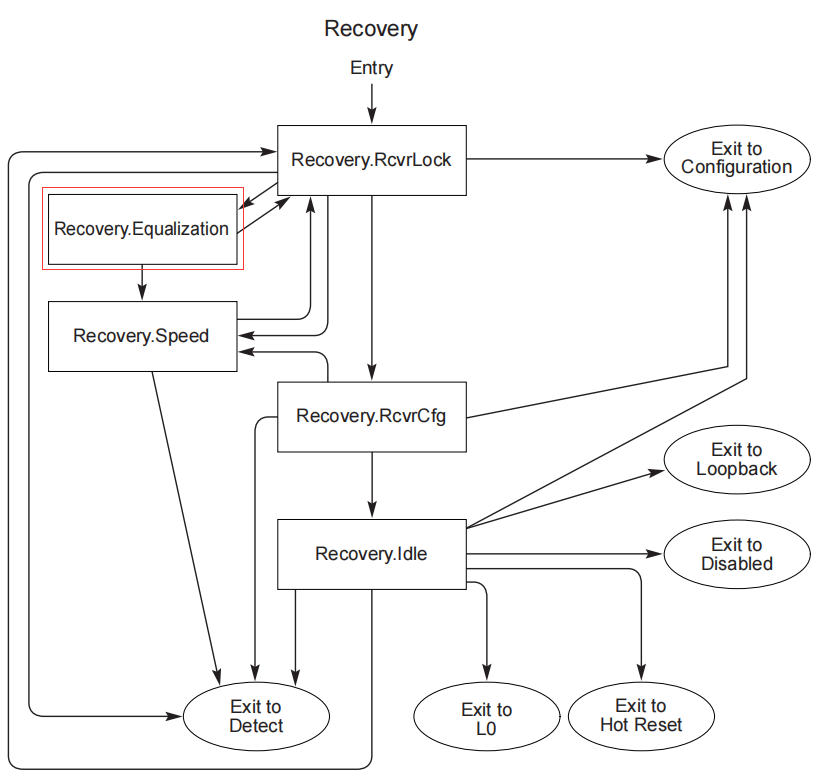
Figure 4: Transitions between Recovery substates (Source: PCI-SIG)
Phase 0
This is the first stage of link equalization. The DSP sends the required transmission endpoint preset values to the USP for each lane, which are conveyed through Training Sequence 2 (TS2). Upon receiving the request from the DSP, the USP increases the data transmission rate of the link to Gen3 (8 GT/s) and sends back a Training Sequence 1 (TS1) containing the received preset values. Once the Gen3 connection is established, the link equalization enters Phase 1.
Phase 1
The same TS1 is repeated regardless of link quality to ensure that DSP receives the correct preset values. This is done to prime the link for the exchange of TS1 and the subsequent stages of link fine-tuning. Once the link achieves a Bit Error Rate (BER) of ≤10e-4, the link equalization enters Phase 2.
Phase 2
The DSP adjusts the USP's preset values by sending equalization requests through TS1 until the optimal settings are obtained, with the link's BER meeting the requirement of ≤1E-12.
Phase 3
The USP adjusts the DSP's preset values by sending equalization requests through TS1 until the optimal setting link's BER ≤1E-12 is met. The conclusion of Phase 3 also concludes the link equalization process.
However, certain motherboard designs with long channel links may require additional signal conditioning for optimal signal quality. In such cases, repeaters (such as ReDrivers, ReTimers) are used for signal conditioning and to provide high-quality signals between PCIe devices and the Root Complex (a crucial connection between the CPU, storage devices, and PCIe devices). The link will enter the L0 state at the Gen3 rate and maintain stable communication at that rate. For higher transmission rates, the PCIe devices must go through the link equalization process multiple times.
At 8GT/S, the equalization process between the DSP and USP is shown in Figure 5.

Figure 5: 8GT/s Dynamic Link Equalization Process (Source: PCI-SIG)
At 16GT/s, the equalization process between the DSP and USP is shown in Figure 6.

Figure 6: 16GT/s Dynamic Link Equalization Process (Source: PCI-SIG)
Multiple equalization modes
The traditional approach in PCIe equalization is the full equalization mode, where equalization starts at lower rates that gradually increases until a target rate is reached. However, as the PCIe transmission rate doubles, the number of equalization steps increases, leading to longer processing times and impacts on system performance. To address this, starting from Gen5, PCIe introduced equalization across intermediate rates to reduce equalization time. Additionally, for links with excellent native transmission quality, equalization can be disabled altogether.
Equalization bypass to highest rate
“Equalization bypass to highest rate” mode can only be applied when both devices support and enable this feature. During the link training process, the devices negotiate whether to use this mode in the Configuration state of LTSSM by exchanging TS sequences. If this mode is selected for link training, a single speed change occurs. After the link enters Recovery directly from the L0 state at 2.5GT/s, it switches to the highest rate (32GT/s or above) and undergoes one round of equalization. If equalization fails at the highest rate and subsequent equalization attempts also fail, downgrading should be considered.
No equalization needed
No equalization needed mode can be chosen if both devices support a speed of 32GT/s or higher and the link quality is excellent or if the previous equalization preset values are available locally. This will allow the fastest speed to be achieved without equalization. Instead, devices will negotiate whether to use the “no equalization needed” mode in the Configuration state of LTSSM by exchanging TS sequences.
Determination of the equalization result
For transmission rates of PCIe 3.0 and above, the success of equalization is determined based on the transmission error rate. Adjusting the equalizer coefficients for each lane individually ensures that the transmission error rate on all valid lanes of the link meets the criterion of BER ≤ 1E-12. If this criterion is met within a specific response time, equalization at that speed is considered successful. The maximum response time is defined as 500 ms in the Base specification¹ and 1 μs in the CEM specification². From a procedural perspective, equalization is considered successful when LTSSM.Equalization completes the transition from Phase 0 to Phase 3 and proceeds to the next state.
PCIe link training and signal equalization in a nutshell
PCIe is a widely used high-speed serial computer expansion bus standard. During link training, PCIe devices establish connections between the Root Complex and other devices. Initially, PCIe devices operate at Gen1 (2.5GT/s) transmission rate. However, if all connected devices support Gen3 (8GT/s) or higher, a link equalization process is initiated to establish a higher-speed PCIe link. This process involves four stages of adjustment to ensure stable data transmission at the highest supported rate while maintaining a low transmission error rate of BER ≤ 1E-12.
Test your PCIe products at GRL
At GRL, we have an extensive background in PCIe technology and supporting adopters across the ecosystem. Our team's deep industry knowledge positions us as trusted experts in PCIe compliance testing. We offer comprehensive testing for PCIe 6.0, 5.0, 4.0, and earlier Base (ASIC) and CEM (System) Specifications. With GRL as your testing partner, you can trust us to deliver accurate results, streamline your testing process, and help you bring your PCIe devices to market with confidence.
References
- PCI Express Base Specification Revision 4.0 Version 0.7
- PCI Express Architecture PHY Test Specification, Revision 4.0, Version 1.0
- PCI Express Architecture PHY Test Specification, Revision 3.0
- PCI Express Architecture PHY Test Specification, Revision 5.0, Version 1.0
.png)