Granite River Labs, GRL
Wing Tseng 曾威華
What Is Double Data Rate (DDR) and How Does It Improve Memory?
This article will provide an overview of DDR by:
- Breaking down memory into DRAM and SRAM
- Briefly touching upon the evolution from SDRAM to DDR5
- Highlighting main upgrades from DDR4 to DDR5
- Describing the five main DDR signal types
- Highlighting the main differences between DDR and LPDDR
To understand Double Data Rate (DDR), one must first understand how memory functions in the major 3C products (computer, communication, and consumer electronics). Memory is a temporary data storage area where programs are safekept while a device is in operation. This storage space enables the device to switch between programs by retrieving stored information rapidly, creating a smoother and more efficient user experience. DDR technology improves the data retrieval process by improving data transfer rates and optimizing power efficiency, making it a popular choice for modern devices since its inception in 2000.
What are DRAM and SRAM?
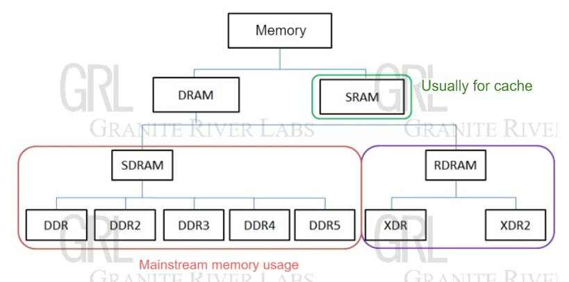
Figure 1: Chart of DRAM and SRAM memory sub-categories further broken down into SDRAM and RDRAM standards
Device storage memory can be broadly broken down into two categories: Dynamic Random Access Memory (DRAM) and Static Random Access Memory (SRAM). While there are several other types of RAM, such as Rambus DRAM (RDRAM), Fast Page Mode RAM (FP RAM), and Extended Data Out RAM (EDO RAM), they are considered to be rare memory types that do not receive widespread usage. As such, we will not discuss them in detail in this article.
Both DRAM and SRAM are considered to be volatile memories, which means that they require constant power supply to retain data. While DRAM uses capacitors and transistors, SRAM primarily uses flip-flops and is commonly deployed in cache. In recent years, a type of DRAM known as Synchronous Dynamic Random Access Memory (SDRAM) has risen to become the most prominently used DRAM. SDRAM is also widely known as Single Data Rate SDRAM (or SDR SDRAM), and enables SDRAM block frequencies to exceed 100MHz by synchronizing the memory clock and CPU processor, thereby bringing data transmission closer to real time.
The main differences between DDR and SDRAM become apparent once it is made clear that DDR actually stands for DDR SDRAM, or Double Data Rate SDRAM, which hints at how DDR was designed to hasten the data transfer rate by two times. The following table covers the technical differences between the two memory technologies in greater detail:
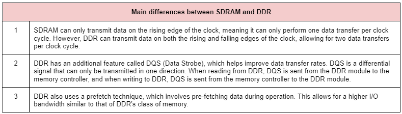
Table 1: Three defining differences that separate SDRAM and DDR
The history of how DDR specifications have evolved from SDRAM to DDR5
DDR specifications are developed and set by the Joint Electron Device Engineering Council (JEDEC), which is also known as the JEDEC Solid State Technology Association.
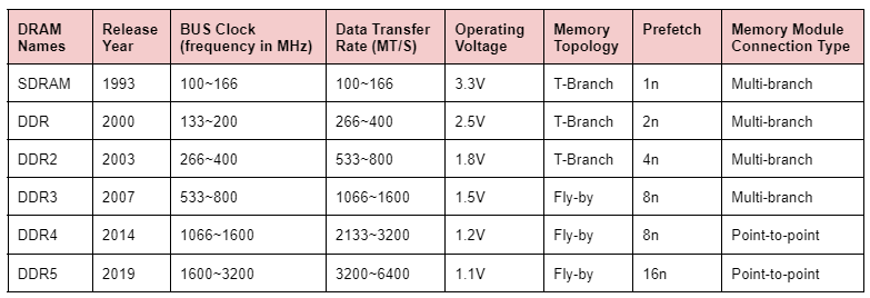
Table 2: Specifications of DDR throughout history
DRAM specifications throughout history have advanced to produce higher transmission rates and lower operating voltages. One significant milestone came during the introduction of DDR3, which replaced T-branches used in DDR2 and prior with a fly-by series that enabled more efficient transmission of command/address and clock signals to each memory chip.
Another groundbreaking development came during DDR4, memory connections formed using a “multi-branch” approach that connected CPU processors to multiple memory chip controllers were replaced by individual channels that established “point-to-point” connections with the CPU. This direct channel approach enhanced memory access efficiency and reduced power consumption, resulting in greater system performance.
How DDR5 improves upon DDR4 RAM memory
DDR5’s development has been highly anticipated among 3C manufacturers due to its promised potential to create denser memory sticks with higher bandwidth levels. DDR5 enables this by raising memory chip capacity from 16-gigabits to 64-gigabits, as well as supporting stacks of up to eight dies on each chip, allowing it to maximize capacity at 2TB per module.
Although JEDEC’s specified data rate range reaches DDR5-3200, the data rates of mainstream DDR5 products tend to start at approximately DDR5-4800. This is a significant increase from DDR4’s data rate range of DDR4-1600 to DDR4-3200. In addition, DDR5 memory modules are equipped with two independent 32-bit channels, compared to DDR4’s single 64-bit channel.
In terms of power efficiency, DDR5 brings DDR4’s operating voltage of 1.2V down to 1.1V. At the time of writing, all 1.1V memory kits conform to JEDEC’s specified timings.
But unlike DDR4 which introduced more pins, DDR5 still sticks to the same 288 pin arrangement. The only change here lies in different pinouts that alter the notch position to prevent newer users from mistakenly inserting a DDR5 memory module into a DDR4 slot, or vice-versa.
What are the five main DDR signal types?
DDR signals work together to ensure that data is transferred accurately and efficiently between the memory controller and module. The five main DDR signal types, clock, data, data strobe, control, and access, play synergistic roles in data storage, retrieval, transfer, verification, and more. The following table talks about each signal in more detail:
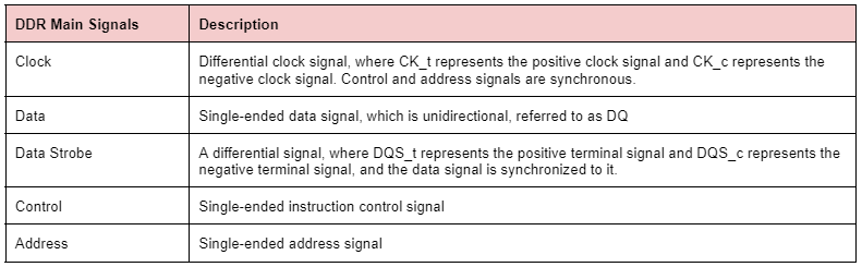
Table 3: Description of the main DDR Signal Types
DDR is designed to function using a half-duplex operation, where read and write memory cycles occur on the same signal trace, but during different time intervals. It is therefore important for manufacturers to differentiate between read and write cycles for accurate DDR test analysis.
Because DDR read and write cycles are not aligned, differential strobe signals (DQS) are required to latch onto data (DQ) during stable high or low phases. Note that DQ and DQS are in-phase during read cycles, and have a 90-degree phase difference during write cycles.
Currently, DDR types can be roughly divided into the following three categories:
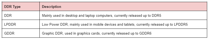
Table 4: DDR types and categories
DDR vs LPDDR
LPDDR is a low-power, synchronous, dynamic random-access memory designed specifically for mobile devices such as smartphones and tablets. LPDDR differs significantly from DDR in terms of performance, battery life, and hence, data transfer.
For example, devices equipped with LPDDR will be expected to use less power than equivalent DDR devices. On the flipside, DDR devices should perform better than LPDDR devices on memory tests with the same benchmarks.
It is therefore important to understand the differences between DDR and LPDDR operating voltage values, which have evolved with each new installation:
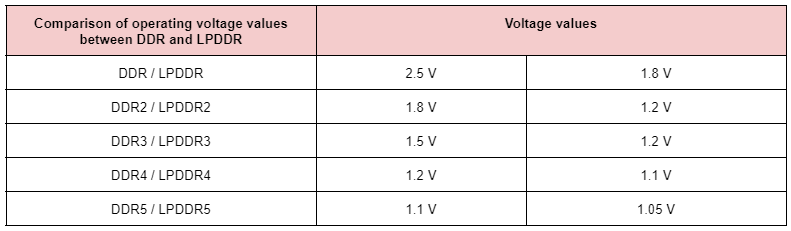
Table 5: Operating voltage values of DDR and LPDDR
Get your DDR products tested by GRL
Looking for comprehensive and reliable DDR compliance testing for your product development needs? Whether you’re looking for DDR compliance testing services covering specifications from DDR to DDR5 and LPDDR to LPDDR5, GRL’s experts have the knowledge and equipment to deal with them all. Contact us today and receive a specialized consultation to see how you can ensure that your products meet the latest industry standards.
References
- Low Power Double Data Rate SDRAM Standard (LPDDR), JESD209B, February 2009
- Low Power Double Data Rate 2 (LPDDR2), JESD209-2F, April 2011
- DDR3 SDRAM Standard, JESD79-3F, July 2010
- Low Power Double Data Rate 3 (LPDDR3), JESD209-3C, August 2013
- DDR4 SDRAM, JESD79-4, September 2012
- Low Power Double Data Rate 4 (LPDDR4), JESD209-4B, November 2015
- Low Power Double Data Rate 5 (LPDDR5), JESD209-5, February 2019
- DDR5 SDRAM, JESD79-5, July 2020