Granite River Labs, GRL
By Fred Chen – Technical Engineer, GRL (Taipei)
Secure Digital Memory Cards (SD Cards) are used widely in portable consumer electronic products, such as digital cameras, laptops, tablet PCs, mobile phones, handheld game machines, and e-books. Since the launch of Version 1.01 in 2000, SD Card storage capacity has grown from 8MB to128TB, and access speeds have increased from 12MB/s to 985MB/s.
Capacities & Specifications
SD Cards are now available in four standard storage capacities. The names, trademarks and file systems used are listed in Table 1 (below).
 |
Standard Capacity SD Memory Card (SDSC) |
Maximum storage capacity is 2GB. Supports the FAT 12 and FAT 16 file systems. |
 |
High Capacity SD Memory Card (SDHC) |
Storage capacity ranges from 2GB to 32GB. Supports the FAT 32 file system. |
 |
Extended Capacity SD Memory Card (SDXC) |
Storage capacity ranges from 32GB to 2TB. Supports the exFAT file system. |
 |
Ultra Capacity SD Memory Card (SDUC) |
Storage capacity ranges from 2TB to 128TB Supports the exFAT file system. |
Table 1: Standard SD Card Storage Capacity Trademarks and File System Details
While the latest SD Card specification is Version 8.0, most of the cards currently on the market use Version 3.01 or 4.0. Accordingly, this overview will focus on SD 3.01 and SD 4.0.
One obvious difference between SD 3.01 and SD 4.0 is seen in the way their pins are laid out [see Figures 1 & 2]. However, there are other technical and performance differences.
For example, SD 3.01 supports a default bus speed mode (12.5MB/s) and a high-speed mode (25MB/s), with a working voltage of 3.3V. It also supports Ultra High Speed bus Interfaces (UHS-I), ranging from SDR25 (25MB/s) to SDR50 (50MB/s), SDR104 (104MB/s), and DDR50 (50MB/s) all of which use a working voltage of 1.8V.
Single Data Rate (SDR) means that data (one bit) can be retrieved once during a cycle. An SD Card has four data lines, so it can transmit four bits per cycle. Therefore, if the maximum transmission rate is 50MB/s, the upper frequency limit is 100MHz.
Double Data Rate (DDR) means that data can be retrieved twice per cycle, enabling 8 bits to be transmitted. In this case, the maximum transmission rate is equal to the upper frequency limit.
In SDIO (Secure Digital Input Output) mode, UHS-I can use four data lines for transmission (4-bits of data) via Pins 1, 7, 8, and 9 (DATA0 - DATA3). If the four-line transmission is not supported, a single line (Pin 7, DATA0) is used. Pin 2 is a command line (CMD) for transmission and communication between HOST and DEVICE. Pin 5 is the clock line (CLK). For details, please refer to Table 2 below.
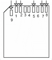
Figure 1. SD 3.01 Pin Design
| Pin | Name | Description |
| 1 | CD/ DAT3 | Card Detect/ Data lane3 |
| 2 | CMD | Command/Response |
| 3 | VSS1 | Supply Voltage Ground |
| 4 | VDD | 3.3V Supply Voltage |
| 5 | CLK | Clock |
| 6 | VSS2 | Supply Voltage Ground |
| 7 | DAT0 | Data lane0 |
| 8 | DAT1 | Data lane1 |
| 9 | DAT2 | Data lane2 |
Table 2. SD 3.01 Pin Description
SD 4.0 Cards use the UHS-II bus interface, which features two rows of pins rather than the single row found in UHS-I. The original single row of pins is compatible with the preset, high-speed, and UHS-I transmission modes. Table 2 shows the details of all the pins used by the UHS-II interface, which transmits signals in half-duplex and full-duplex mode. Providing two routes for signal transmission enables much faster bus speeds than UHS-I.
In full-duplex mode, one route is distributed downward (from host to memory card), and the other route upward (from memory card to host). In this mode, the data packets are transmitted in two directions at the same time, with a one-way transmission rate of 156MB/s, doubled in two-way transmission to 312MB/s. In half-duplex mode, the two routes transmit the data in the same direction.
 Figure 2. SD 4.0 Pin Design
| Pin | Name | Description |
| 4 | VDD1 | 2.7V to 3.3V |
| 7 | RCLK+ | Clock input |
| 8 | RCLK- | Clock input |
| 10 | VSS3 | Supply Voltage Ground |
| 11 | D0+ | Input in default |
| 12 | D0- | Input in default |
| 13 | VSS4 | Supply Voltage Ground |
| 14 | VDD2 | 1.7V to 1.95V |
| 15 | D1+ | Input in default |
| 16 | D1- | Input in default |
| 17 | VSS5 | Supply Voltage Ground |
Table 3. SD 4.0 Pin Description
SD Card Physical Layer Testing
UHS-I
During signal transmission, DATA has Input timing and Output timing parameters created by writing and reading, while Clock (CLK) has Input timing in one direction. The signal transmission quality of a product can be ensured by measuring the CLK and DATA signals to verify that the parameter values conform to the Specification set out by the SD Association.
The Clock Threshold (V_CT) of the clock signal is defined as 0.975V, and the CLK cycle can be obtained by establishing a reference point through V_CT, as shown in Figure. 4. The Input High Voltage (V_IH) and the Input Low Voltage (V_IL) are defined by the developer within a specified range. The V_IH ranges from 1.27V to 2.00V, and the V_IL ranges from V_SS-0.30V to 0.58V. The CLK (t_CR) rise time and the CLK (t_CF) fall time can be calculated from the interval between V_IH and V_IL. The quality of the signal is determined by measuring the cycle, rise time, fall time, and duty ratio of CLK and comparing the results with the SD Association specifications.
.png?width=919475&name=%E5%9C%96%E7%89%871%20(2).png) Figure 4. Figure 4. UHS-I Clock (Source: SD Association 3.01 Physical Layer Specification)
Figure 4. Figure 4. UHS-I Clock (Source: SD Association 3.01 Physical Layer Specification)
With V_CT as the reference point, the DATA signal marks the interval between V_IH (max) of V_IL (min) [See Figure. 5] as the set-up time (t_IS) and hold-time (t_IH) of DATA. If the working voltage is too low and the values of V_IH and V_IL defined by the user are too high, the interval marked as set-up time and hold-time will get shorter. This will make it difficult for the product to interpret the logical alignment, so paying attention to the relationship between the two while measuring the Data signal is important.
.png?width=727021&name=%E5%9C%96%E7%89%872%20(1).png) Figure 5. UHS-I Data (Source: SD Association 3.01 Physical Layer Specification)
Figure 5. UHS-I Data (Source: SD Association 3.01 Physical Layer Specification)
UHS-II
Physical layer testing for UHS-II is carried out in full-duplex mode. Transmitter Testing and the Receiver Testing for two signal pairs (D0, D1) is conducted by switching the product into Forward / Backward Loopback mode. The Transmitter Test (Tx) is used to confirm the quality of the signals transmitted by the product, while the Receiver Test (Rx) confirms the product’s ability to correctly interpret the signals received.
The product is tested at two data rates, namely Range A and Range B. Range A is 390Mbps - 780Mbps, calculated using the formula of CLK frequency (26MHz - 52MHz specified in the UHS-II product specification) multiplied by 15 times the Ratio (Data rate/CLK frequency). Range B is 780Mbps - 1560Mbps, calculated from the CLK frequency multiplied by 15 times the 30 Ratio (Data rate/CLK frequency).
(1)Transmitter Test
When testing the D0 signal pair, the Signal Generator sends a test pattern (CLK and PRBS 2^7-1) to the D1 signal pair, and the signal received by D1 is first transmitted to D0 via Forward Loopback mode, and then connected to the oscilloscope where the captured waveform is analyzed [Figure 6].
When testing the D1 signal pair, the product should be switched to Backward Loopback mode, which will input the signal to D1 from D0, then output it to the oscilloscope [Figure 7]. Table 3 shows the items and specifications for Tx analysis. The lowest rise time and fall time values are set. Phase difference and voltage must be within a certain range, according to differential voltage and common-mode voltage specifications.
.png?width=516663&name=%E5%9C%96%E7%89%873%20(3).png)
Figure 6. UHS-II D0 Signal Pair Transmitter Test Process
.png?width=1058852&name=%E5%9C%96%E7%89%874%20(3).png)
Figure 7. UHS-II D1 Signal Pair Transmitter Test Process
.png?width=392120&name=6%20(1).png) Table 4. UHS-II Transmitter Test Items and Criteria
Table 4. UHS-II Transmitter Test Items and Criteria
(2) Receiver test
The receiver test is designed to determine whether a product can accurately receive signals.
During transmission, factors such as PCB circuit loss and ambient temperature can cause signal attenuation. Therefore, it is important to ensure that the receiver is able to interpret the attenuated signal accurately.
To simulate attenuation, a certain amount of jitter is added to the source signal transmitted to the product (using PRBS 2^7-1 test pattern) during the receiver test. The receiver receives the signal in Loopback mode and sends it back to the Error Detector. No bit errors are allowed.
Table 4 shows the specific amount of jitter to be added when measuring two jitter frequency points (0.234MHz and 2.34MHz) under different transmission rates (390Mbps~1.56Gbps) and the 3*1011 bits to be tested at each point.
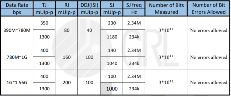 Table 5. UHS-II Receiver Test Criteria
Conclusion
The SD Card UHS-I interface supports SDR25, SDR50, SDR104, and DDR50 transmission modes, with a working voltage of 1.8V, and signal quality is determined by measuring the DATA and CLK parameters on the physical layer.
SD Card UHS-II is compatible with UHS-I, and in full-duplex mode signal rates can reach 1560 Mbps. In physical layer transmitter and receiver testing, both signal pairs (D0, D1) can be tested by putting the product into Loopback mode.
References
- Part 1 UHS-II PHY Test Guideline Ver.1.00 Final 140714
- Part 1 Physical Layer Specification Ver5.10 Final 161101
- Part 1 UHS-II Addendum Ver1.02 Final 140528
- Format of SD Specification
Author
Fred Chen – Technical Engineer, GRL (Taipei)
Fred has more than four years of testing experience at GRL and is familiar with testing specifications for a variety of connectivity technologies, including Displayport™, SD Card, and Thunderbolt. His day to day responsibilities include assisting customers in obtaining product certification. He also lectures on testing and certification, as well as writing technical articles for GRL.